new material

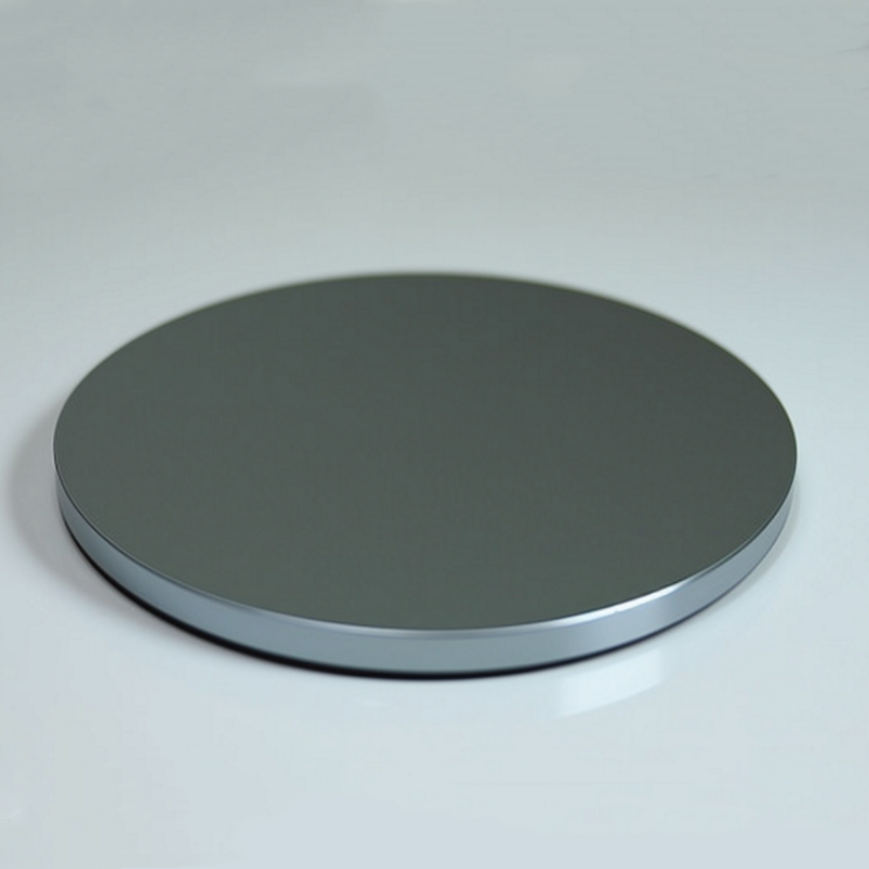


Product Overview
High purity silicon targets are made from 5N-grade silicon materials through precision processing techniques. These targets have a deep gray appearance and exhibit high thermal conductivity and excellent physical properties. Silicon has a melting point of 1414°C and a boiling point of 3265°C, offering excellent high-temperature resistance and a high thermal conductivity coefficient. These properties make high purity silicon targets highly effective for use in microelectronics, optics, and thin-film deposition, especially in reactive magnetron sputtering techniques to deposit high-quality dielectric layers (such as SiO₂, SiN, etc.).
Key Features
- High Purity: Purity of 99.999%, ensuring superior quality and stability.
- Excellent Thermal Conductivity: With a thermal conductivity of 149 W·m⁻¹·K⁻¹, it is ideal for high-temperature applications.
- Customizable: Can be tailored to different sizes and shapes as per customer requirements.
Applications
- LCD Transparent Conductive Glass: Used to deposit transparent conductive layers for LCD displays.
- Low-E Glass for Buildings: Enhances the thermal insulation performance of glass.
- Microelectronics Industry: Used for the deposition of semiconductor devices and thin-film electronic materials.
- Optical Applications: Widely used for the deposition of optical films, such as coatings for optical devices.
- Magnetron Sputtering: Used in the deposition of dielectric layers like SiO₂ and SiN.
| Element | Measured Value | Standard Value | Unit | Element | Measured Value | Standard Value | Unit | Element | Measured Value | Standard Value | Unit | |
| Li | <0.001 | ppm | Zn | <0.05 | ppm | Pb | <0.01 | ppm | ||||
| B | 0.92 | ppm | Ga | <0.05 | ppm | Bi | <0.01 | ppm | ||||
| F | <1 | ppm | Ge | 0.25 | ppm | Y | <0.01 | ppm | ||||
| Na | <0.01 | ppm | As | 0.23 | ppm | Th | <0.005 | ppm | ||||
| Mg | <0.005 | ppm | Se | <0.01 | ppm | Er | <0.005 | ppm | ||||
| Al | 0.03 | ppm | Zr | <0.01 | ppm | Ru | <0.01 | ppm | ||||
| Si | Matrix | wt% | Nb | <0.01 | ppm | Rb | <0.01 | ppm | ||||
| P | 42 | ppm | Mo | <0.01 | ppm | Sr | <0.01 | ppm | ||||
| Cl | <0.05 | ppm | Pd | <0.01 | ppm | Sc | <0.001 | ppm | ||||
| K | <0.05 | ppm | Ag | <0.01 | ppm | Be | <0.001 | ppm | ||||
| Ca | <0.05 | ppm | Sn | <0.01 | ppm | Rh | <0.01 | ppm | ||||
| Ti | <0.005 | ppm | Sb | <0.005 | ppm | Cd | <0.05 | ppm | ||||
| V | <0.005 | ppm | Ba | <0.01 | ppm | |||||||
| Cr | <0.01 | ppm | Hf | <0.005 | ppm | |||||||
| Mn | <0.005 | ppm | Ta | Source | ppm | C | ppm | |||||
| Fe | 0.19 | ppm | W | <0.05 | ppm | S | <0.05 | ppm | ||||
| Co | <0.005 | ppm | Pt | <0.01 | ppm | O | ppm | |||||
| Ni | <0.01 | ppm | Au | <0.1 | ppm | N | ppm | |||||
| Cu | <0.03 | ppm | Hg | <0.01 | ppm | H | ppm |