new material

Copper nanoclusters provide optimized fluorescence properties, superior catalytic efficiency, and enhanced biocompatibility. Designed for advanced applications, they ensure efficient dispersion, extended durability, and high-performance adaptability.

Product Overview
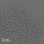
Copper nanoclusters are composed of a few to several hundred copper atoms, positioned between nanoparticles and molecular compounds. They exhibit unique electronic and optical properties. Copper, being a low-cost, environmentally friendly, and low-toxicity material, is widely used in industrial fields. Copper nanoclusters offer enhanced photostability and environmental friendliness, making them more suitable for trace-level detection compared to organic dyes and semiconductor quantum dots.
Key Features
- Fluorescent Properties: The particle size of copper nanoclusters is close to the Fermi wavelength of electrons, giving them unique fluorescent properties. This makes them valuable in biological imaging, sensing, and optoelectronic devices.
- Biocompatibility: Copper nanoclusters exhibit excellent biocompatibility with low or non-toxicity, making them suitable for biomedical applications.
- Water Solubility: The good water solubility of copper nanoclusters enables easy transmission and application within biological systems.
- Photostability: Copper nanoclusters have superior photostability compared to other fluorescent materials, maintaining their fluorescence over extended periods of light exposure.
Applications
- Biomedical: Copper nanoclusters are ideal for biological imaging, cell labeling, and cancer immunotherapy. Their fluorescence properties make them excellent materials for imaging, while their biocompatibility ensures safety in medical applications.
- Environmental Protection: Copper nanoclusters can be used as probes to detect organic pollutants, heavy metal ions, and other contaminants in the environment.
- Petrochemical: In the petrochemical industry, copper nanoclusters participate in catalytic processes such as redox reactions, hydrogen evolution reactions, and CO₂ reduction reactions.
- Optoelectronic Devices: Thanks to their fluorescent properties, copper nanoclusters are used in the fabrication of optoelectronic devices such as LEDs and photodetectors.
| Item | Parameter |
| Concentration | 0.05 mg/mL |
| Solvent | Water |
| Diameter | 1-10 nm (HRTEM) |
| Appearance | Colorless transparent solution |
| Stabilizer | Glutathione (GSH) |