new material
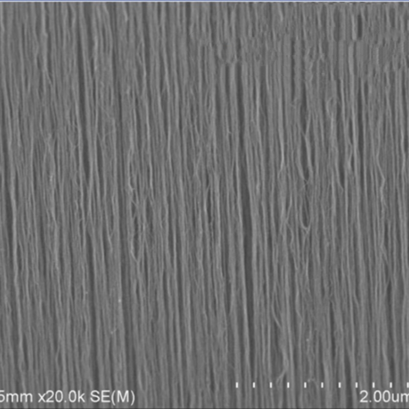
Carbon nanotube vertical array on silica substrate provides optimized electrical conductivity, superior thermal stability, and enhanced structural alignment. Designed for advanced applications, it ensures efficient charge transport, extended durability, and high-performance adaptability.

Product Overview
The Carbon Nanotube Vertical Array on Silica Substrate is an innovative material with high thermal conductivity and mechanical strength. It is produced by growing carbon nanotube vertical arrays on a silica substrate and then transferring them to a target substrate while maintaining the structural integrity. This transfer process preserves the outstanding performance of the array, making it suitable for a variety of applications, including electronic device cooling, electrochemical sensors, and more.
Key Features
- Array Integrity Preservation:The transfer process retains the original ordered structure and morphology of the carbon nanotube array, ensuring its thermal conductivity and mechanical strength.
- Enhanced Application Flexibility:By transferring to different target substrates, the material’s application scope is expanded across various fields.
Applications
- Electrode Materials:The carbon nanotube arrays have excellent conductivity and high surface area, making them ideal for use as electrode materials in lithium-ion batteries and supercapacitors, enhancing energy storage performance.
- Electronic Devices:Due to their low threshold voltage, high emission current, and good stability, carbon nanotube arrays can be used as electron sources in cold cathode X-ray tubes and field emission scanning electron microscopes.
- Thermal Interface Materials:The axial thermal conductivity of the carbon nanotube arrays makes them ideal for use as thermal interface materials, enhancing heat dissipation efficiency in electronic components and improving device stability and longevity.
| Technical Parameter | Value |
| Diameter | 3-10 nm |
| Purity | 98% |
| Height | 100-1000 μm |
| Density | ≤0.3 g/cm³ |
| Specific Surface Area | ~20 m²/g |
| Conductivity | 103 S/m |

")