new material
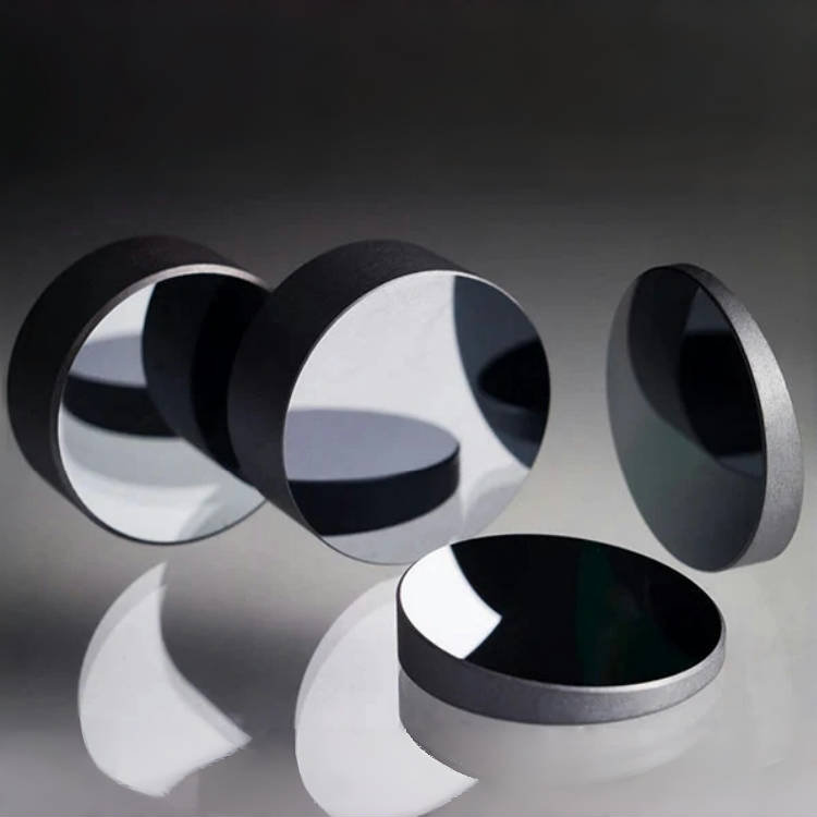
Czochralski silicon (straight pull silicon) is a high-purity semiconductor material produced using the Czochralski method, which enables precise control over crystal growth and structural uniformity. Known for its superior electrical properties, excellent thermal stability, and optimized charge carrier mobility, this material is widely used in semiconductor fabrication, optical components, photovoltaic applications, and scientific research, ensuring reliable performance in advanced electronic and photonic systems.

Product Overview:
Czochralski silicon (or straight pull silicon) is a high-quality silicon single crystal material produced using the Czochralski method. In this process, polycrystalline silicon is melted, and a seed crystal is used to grow a single crystal with a highly ordered atomic structure. Due to its high purity and density, Czochralski silicon is widely used in the manufacturing of semiconductor devices and integrated circuits. The production process is strictly controlled to ensure that the material's optical and mechanical properties meet high standards, making it a key foundational material in many high-tech applications.
Key Features:
- Excellent Optical Transmittance:Shows good transmission in the infrared wavelength range, especially in the 3-5μm band, making it suitable for infrared optical systems.
- High Mechanical Performance:With a high Young's modulus and hardness, it maintains stable performance even under significant pressure and thermal changes.
- Outstanding Thermal Properties:It has a low coefficient of thermal expansion, high specific heat, and good thermal conductivity, ensuring stable optical performance under varying temperature conditions.
- Thermal Stability:Demonstrates high Debye temperature and Poisson's ratio, offering excellent thermal stability and elasticity, making it suitable for high-temperature applications.
- High Purity:With low impurity content, Czochralski silicon ensures excellent performance, ideal for high-precision optical and electronic applications.
Applications:
- Semiconductor Industry:Primarily used for manufacturing integrated circuits and semiconductor devices, Czochralski silicon is one of the core materials in modern electronics.
- Optical Systems:As a substrate for infrared transmissive lenses and mirrors, it is widely used in infrared optical systems.
- Lasers and Optical Fiber Communication:Suitable for high-precision optical components used in lasers, optical communication devices, and other optical instruments.
- Energy Sector:Used in the manufacturing of solar cells for the photovoltaic industry, contributing to the development of green energy applications.
- Research and High-Tech Fields:Due to its excellent optical and thermal properties, it is widely used in scientific research and high-precision optical measurement instruments.
| Optical Property | Value |
| Transmission Range | 1.2-15 μm |
| Refractive Index | 3.41776 @ 10μm |
| Reflection Loss | 46.1% @ 10μm |
| Structure | Single crystal, synthetic |
| Cleavage Planes | <111 |
| Physical Property | Value |
| Density | 2.33 g/cm³ |
| Melting Point | 1414 ℃ |
| Thermal Conductivity | 163 W/(m·K) @ 313K |
| Thermal Expansion | 2.6 × 10⁻⁶/K @ 293K |
| Knoop Hardness | 1100 kg/mm² |
| Specific Heat Capacity | 712.8 J/(kg·K) |
| Dielectric Constant | 13 @ f = 9.37 GHz |
| Young's Modulus | 130.91 GPa |
| Shear Modulus | 79.92 GPa |
| Bulk Modulus | 101.97 GPa |
| Poisson's Coefficient | 0.266 |
| Chemical Property | Value |
| Solubility | Insoluble |
| Molecular Weight | 28.09 g/mol |
| Property | Value |
| Material Name | CZ Silicon |
| Available Size | 3-300mm |
| Growing Method | CZ |
| Type | N-type, P-type |
| Transmittance Range | 1-10μm |
| Crystal Structure | Monocrystalline |
| Orientation | <100>, <111>, <110> |
| Blank Shape | Round, rectangular, wedge, lens, step drilled, special-shaped |
| Report | Compliance with ROHS and REACH reports |
 Diode")
")